Difference between revisions of "Routing Fabric"
| (One intermediate revision by one other user not shown) | |||
| Line 3: | Line 3: | ||
AXIOM Beta mainly consist of one MicroZed ZYNQ board with two MachXO2 FPGAs and 4K camera sensor. The MicroZed is a FPGA-ARM hybrid processing board and it is the main board of the AXIOM Beta. All the other components are connected to the main board. | AXIOM Beta mainly consist of one MicroZed ZYNQ board with two MachXO2 FPGAs and 4K camera sensor. The MicroZed is a FPGA-ARM hybrid processing board and it is the main board of the AXIOM Beta. All the other components are connected to the main board. | ||
[[File:PCB-Stack-Concept-V03-022.jpg]] | [[File:PCB-Stack-Concept-V03-022.jpg | 800px]] | ||
Fig.03: PCB Stack | Fig.03: PCB Stack | ||
| Line 18: | Line 19: | ||
There are two of those (Lattice MachXO2) on the Main Board. On each side, called '''Routing Fabric East''' (RFE) and '''Routing Fabric West''' (RFW). Each of the Lattice MachXO2 has a companion PIC microcontroller for bringup and debugging. | There are two of those (Lattice MachXO2) on the Main Board. On each side, called '''Routing Fabric East''' (RFE) and '''Routing Fabric West''' (RFW). Each of the Lattice MachXO2 has a companion PIC microcontroller for bringup and debugging. | ||
[[File:BetaMainboard_0.32_TOP.jpg]] | [[File:BetaMainboard_0.32_TOP.jpg | 800px]] | ||
Fig.02: The top of the main board | Fig.02: The top of the main board | ||
[[File:BetaMainboard_0.32_BOTTOM.jpg]] | [[File:BetaMainboard_0.32_BOTTOM.jpg | 800px]] | ||
Fig.03: The bottom of the main board | Fig.03: The bottom of the main board | ||
[[File:Top.png]] | [[File:Top.png | 800px]] | ||
Fig.04: Top of the main board | Fig.04: Top of the main board | ||
Latest revision as of 08:04, 20 June 2017
Hope you already known about AXIOM Beta, the first FOSS/OH cinema camera. Well then, let’s talk little more about how AXIOM Beta.
AXIOM Beta mainly consist of one MicroZed ZYNQ board with two MachXO2 FPGAs and 4K camera sensor. The MicroZed is a FPGA-ARM hybrid processing board and it is the main board of the AXIOM Beta. All the other components are connected to the main board.
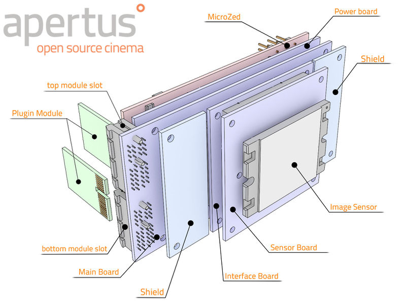
Fig.03: PCB Stack
Above figure shows rough stackup of the boards of AXIOM Beta. The back side is MicroZed, also source FPGA development board featuring the Xilinx ZYNQ as SoC (System on Chip). The purple blue and green boards have been designed by us (includes the main board wich need a driver). The ZYNQ (on the MicroZed) has two hardened ARM cores, which run Linux on the AXIOM Beta. That’s where the scripts are running to program the other FPGAs and PICs.
This device is a 4K cinema movie camera. So the main purpose is to make cinema movies. Some sample footages can be seen in here ([1]).
The ZYNQ is a combination of FPGA and ARM cores, so the image pipeline is implemented in the PL (fabric) part of the ZYNQ while the control software runs on the ARM cores. The ZYNQ mainly connects to the sensor and output plugin modules providing the high speed interfaces to transport 4K video. Only small number of GPIOs are used for ‘lower’ tasks like communicating with the other FPGAs (MachXO2).
The sensor data is transferred from the image sensor to the ZYNQ, processed there and output via one or more of the plugin modules. The sensor gives 4K (4096 x 3072 pixel) images at up to 150 FPS (frames per second) from the sensor. This is a huge amount of data which cannot easily be processed by a CPU, that’s what the PL (FPGA) part is for.
The nice thing about the ZYNQ is that you can boot the ARM cores and load the FPGA configuration from userspace. So changing the FPGA bitstream is only a ‘cat’ to the FPGA dev interface and only takes a fraction of a second. But, this is not the case for the other FPGAs in the system (the Lattice MachXO2).
There are two of those (Lattice MachXO2) on the Main Board. On each side, called Routing Fabric East (RFE) and Routing Fabric West (RFW). Each of the Lattice MachXO2 has a companion PIC microcontroller for bringup and debugging.
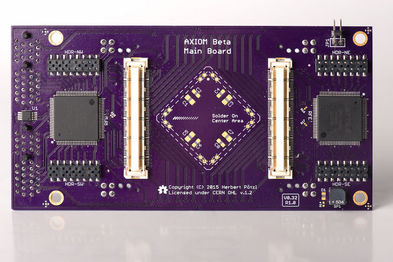
Fig.02: The top of the main board
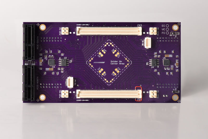
Fig.03: The bottom of the main board
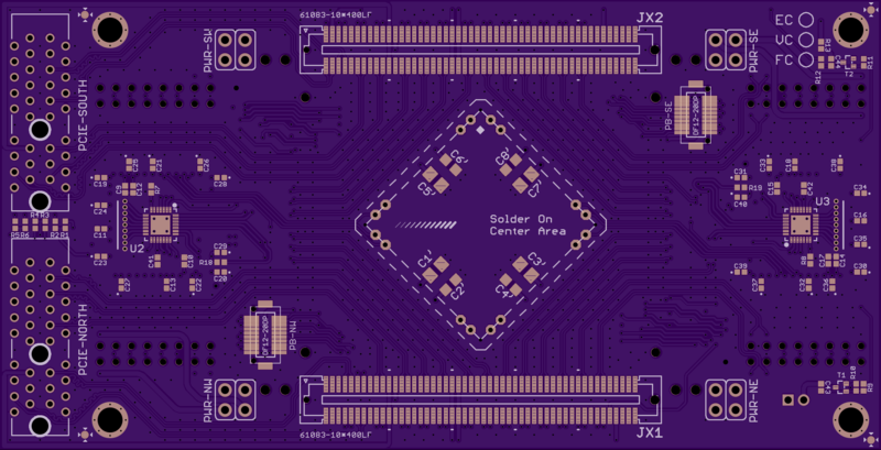
Fig.04: Top of the main board
In the Main Board (https://wiki.apertus.org/index.php/Beta_Main_Board), at the top(Fig.02) you can see the two large Lattice MachXO2. At the bottom (Fig.03 (This is an out dated image)) you can see tiny PICs U3 and U5. They are right below the FPGAs connecting to the JTAG pins and other stuff. On the recent board (Fig.04), you can see we have removed the flash, which right besides the PICs. i.e. U2 and U3 are gone in newer main boards.
The FPGAs can be loaded with a bitstream without ‘programming’ it into the FPGA. Therefore, they don’t need a flash anyway. But MachXO2 also provide an internal flash which can be programmed so that the MachXO2 has its bitstream ready on power up.
When the main board is unprogrammed, there is no code in the PICs and nothing for/in the FPGAs. The PICs are connected via an I2C bus to the PS (ARM cores) part of the ZYNQ. First a small ZYNQ firmware is loaded (via xdev) to allow to ‘abuse’ the I2C bus for programming the PICs. This interface basically transfers the PIC code which was previously compiled on the ARM cores into the PICs. Once that is done, the PICs themselves act as I2C slaves and show up on the I2C bus. Bia those I2C registers, access to the MachXO2 JTAG interface is available. Then the FPGA code for the MachXO2 is uploaded and stored into the flash memory on the devices. Once that is done, the main board is ready to go.
Note that, this process can be repeated anytime during the life of the camera hardware, so it is not something done separately. Also note that for developing software for the MachXO2, the bitstream will not be programmed into the FPGAs, instead it will only be uploaded into their SRAM. This way a new bitstream can be quickly tested without making it permanent. Any debugging for the MachXO2s is currently only feasible via the pin0row mentioned above, i.e. if you attach some cables to the board.
But as the PIC has complete control over the JTAG lines, a software interface on the ARM cores would allow for attaching a JTAG debugger without any cables. And as the AXIOM Beta is designed as development kit for folks interested in working with high speed cameras. Apertus also want to provide convenient way to access and modify all parts of hard and software.
At the moment, Apertus is using python scripts to be precise. But with that, it can’t attach something like OpenOCD to a script. The scripts are not that efficient in communicating with the JTAG interface, so a significant speedup is possible with using a Linux Device Driver.
Basic Set-up of PIC
The Documentation for the PIC16F1718 can be found at [2]
Two IO pins from the FPGA and one GPIO pin (Port extended on different bus) are connected to the programming interface of the PIC16F1718. The two FPGA IOs are connected to RB6 (IC SPCLK) and RB7 (IC SPDAT) of PIC16F1718. The GPIO extended IO is connected to RE3 (#MCLR).
This setup allows to program the PIC via those three connections, with the PIC specific ICSP protocol. Once the PIC is programmed, it uses the two FPGA connections as I2C bus. I.e. RB7 becomes SDA and RB6 become SCL.
The programmed PIC then act as I2C slave with a number of addresses (32). The PIC connects to all relevant programming interfaces of the MachXO2. It also connects to some interfaces for the sensor side, and the plugin interface ( mainly I2C, SPI and some enable pins). The PIC also shares a clock line (dedicated ZYNQ IO) with the Lattice (RA6).
All the pins labeled as *_W or *_E are direct connections between PIC and MachXO2. Networks labeled E_*, W_*, N_* and S_* are controlled from the PIC and used for sensor or plugin interface. The West Routing Fabric (RFW) and the East Routing Fabric (RFE) are the two MachXO2 devices. Currently the python scripts uses the I2C registers on the PIC to control the JTAG lines to the MachXO2.


