Difference between revisions of "Elgato CAM LINK 4K"
| (5 intermediate revisions by one other user not shown) | |||
| Line 1: | Line 1: | ||
This PCB is relevant to the project because [[AXIOM Beta]] generates HDMI content inside its [[Beta Main Board]] FPGA and therefore almost any data can be sent over an HDMI connection. This provides a potential solution to not having control at the HDMI receiver side (recorder manufacturers do all kinds of strange things with the image, e.g. sharpening, colour conversions, etc... and in general only support very specific resolutions/frame-rates. Coincidentally there are also no standards for HDMI. | This PCB is relevant to the project because [[AXIOM Beta]] generates HDMI content inside its [[Beta Main Board]] FPGA and therefore almost any data can be sent over an HDMI connection. This provides a potential solution to not having control at the HDMI receiver side (recorder manufacturers do all kinds of strange things with the image, e.g. sharpening, colour conversions, etc... and in general only support very specific resolutions/frame-rates). Coincidentally there are also no standards for HDMI. | ||
With the Elgato CAM Link 4k it could now become possible to take over control of the receiver side. This opens up a whole world of possibilities with regards to what data could be packed into the HDMI "frame" if it were to be used as a data container. | With the Elgato CAM Link 4k it could now become possible to take over control of the receiver side. This opens up a whole world of possibilities with regards to what data could be packed into the HDMI "frame" if it were to be used as a data container. | ||
| Line 23: | Line 23: | ||
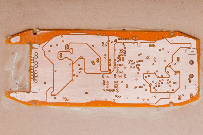
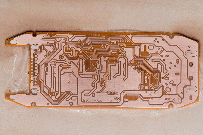
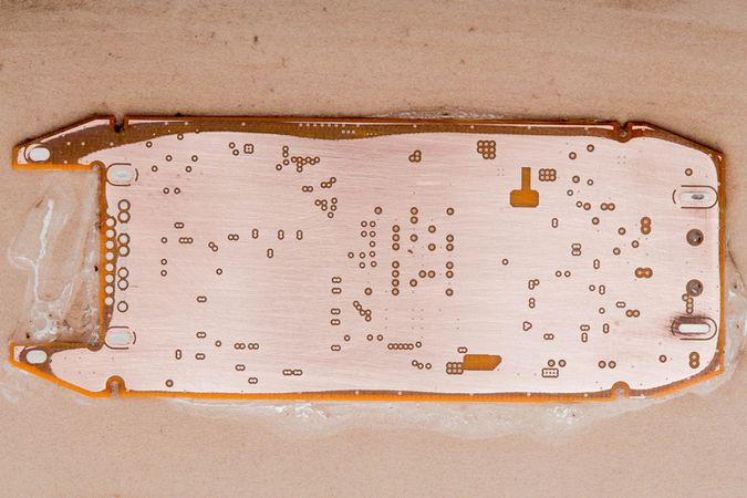
Image:EL_CdWzU8AEtWR_.jpg| PCB Layer 7/8 (flipped) ground plane - Note: 2 cutouts in this plane, that seem to correspond to SW signals of DCDC buck converters. I've never seen that before? Maybe to reduce capacitance on the SW pin? | Image:EL_CdWzU8AEtWR_.jpg| PCB Layer 7/8 (flipped) ground plane - Note: 2 cutouts in this plane, that seem to correspond to SW signals of DCDC buck converters. I've never seen that before? Maybe to reduce capacitance on the SW pin? | ||
Image:EL_CnZjUwAEaASg.jpg| PCB Layer 8/8 (flipped) bottom layer | Image:EL_CnZjUwAEaASg.jpg| PCB Layer 8/8 (flipped) bottom layer | ||
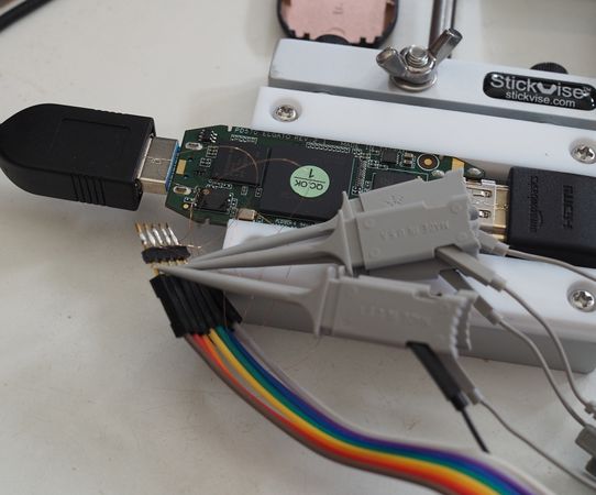
Image:Elgato bodge wires.jpg| Exploring Elgato CamLink4K via oscilloscope. Image from [https://assortedhackery.com/patching-cam-link-to-play-nicer-on-linux/ Assorted Hacking] article on getting the device to play nicer on Linux. | |||
</gallery> | </gallery> | ||
| Line 52: | Line 53: | ||
==Credits== | ==Credits== | ||
* https://twitter.com/GregDavill | * PCB and layer images: https://twitter.com/GregDavill | ||
Latest revision as of 08:42, 7 June 2021
This PCB is relevant to the project because AXIOM Beta generates HDMI content inside its Beta Main Board FPGA and therefore almost any data can be sent over an HDMI connection. This provides a potential solution to not having control at the HDMI receiver side (recorder manufacturers do all kinds of strange things with the image, e.g. sharpening, colour conversions, etc... and in general only support very specific resolutions/frame-rates). Coincidentally there are also no standards for HDMI.
With the Elgato CAM Link 4k it could now become possible to take over control of the receiver side. This opens up a whole world of possibilities with regards to what data could be packed into the HDMI "frame" if it were to be used as a data container.
The device can be purchased from here
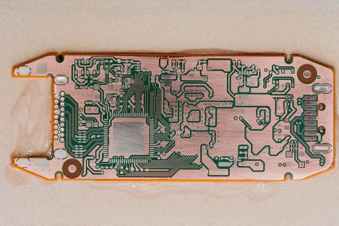
1 PCB
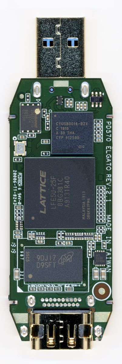
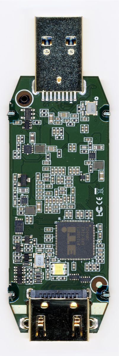
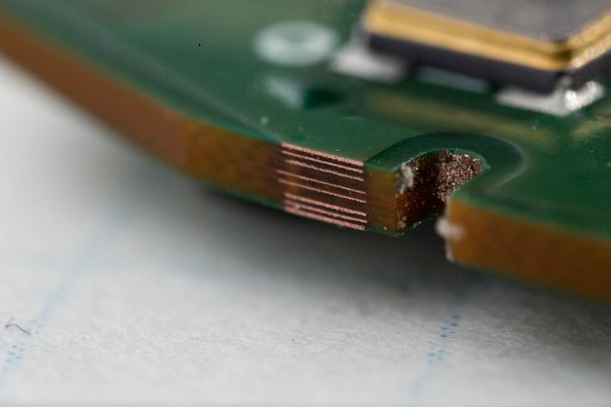
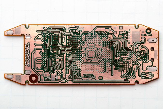
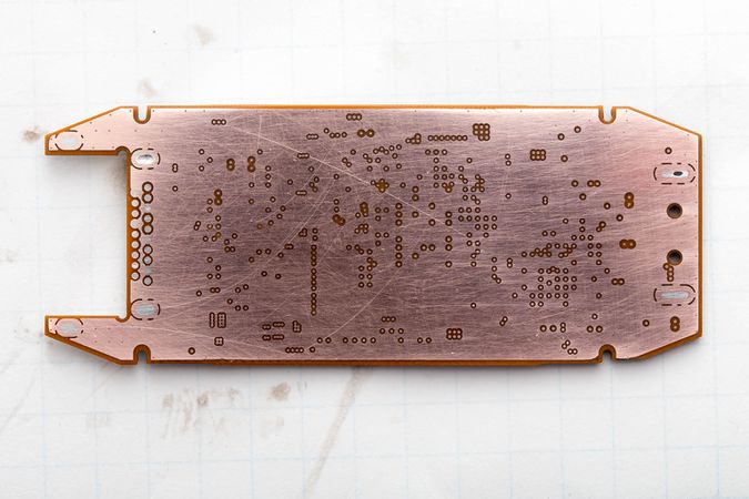
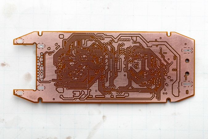
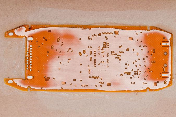
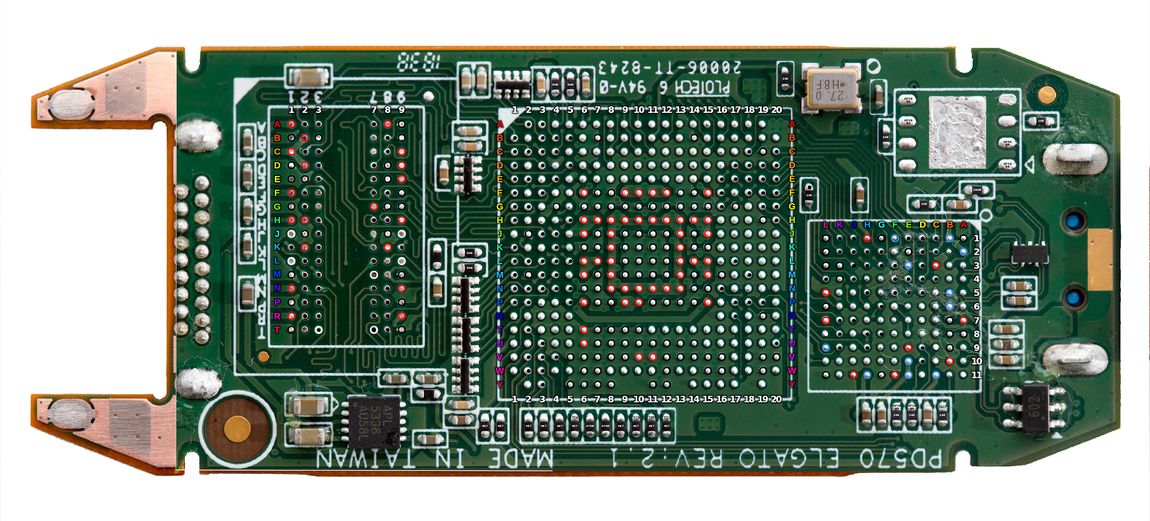
It is reported to be an 8 layer PCB. Probably atleast a 2-3+ HDI.
Exploring Elgato CamLink4K via oscilloscope. Image from Assorted Hacking article on getting the device to play nicer on Linux.
Pinout Mapping (WIP):
2 Firmware
a dump of the SPI communication (and the decoded flash data) can be found here:
- http://vserver.13thfloor.at/Stuff/ELGATO/boot_decode.txt
- http://vserver.13thfloor.at/Stuff/ELGATO/boot.vcd.xz
3 Further files/links
- http://vserver.13thfloor.at/Stuff/ELGATO/
- https://github.com/ktemkin/camlink-re
- Patching my Cam Link 4K to play nicer on Linux - https://assortedhackery.com/patching-cam-link-to-play-nicer-on-linux/
4 Credits
- PCB and layer images: https://twitter.com/GregDavill
