Difference between revisions of "Beta Debug Shield"
From apertus wiki
| Line 18: | Line 18: | ||
See [[Beta Main Board]] for specifics on how shields are utilised and [[AXIOM_Beta/Camera_Structure | Camera Structure]] for how | See [[Beta Main Board]] for specifics on how shields are utilised and [[AXIOM_Beta/Camera_Structure | Camera Structure]] for an overview on how PCBs are stacked. | ||
Revision as of 21:56, 15 January 2020
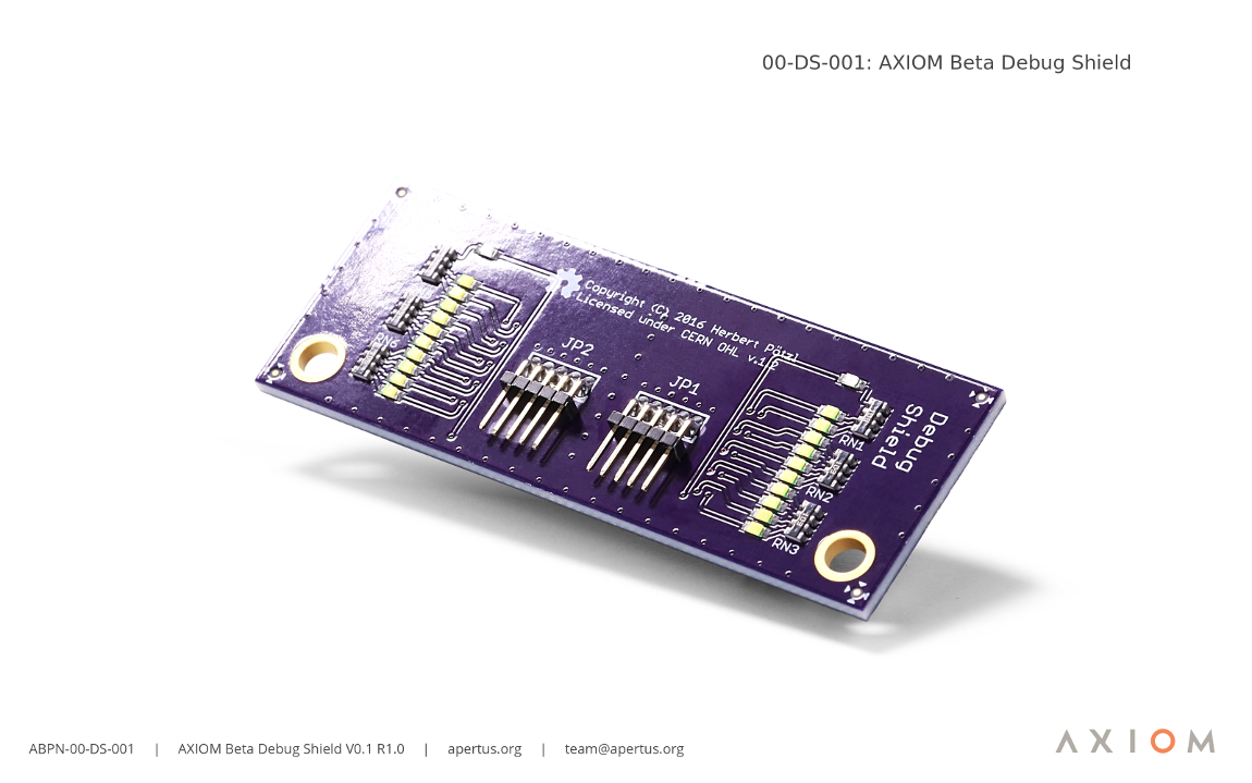
AXIOM Beta features two shield-slots with space for additional connectors going to both east and west sides of the camera. One shield has a slow-speed (200Mb/s) interface and one medium-speed (1Gbit/s) interface connecting to the main processing FPGA. Therefore these shields are perfect for additional future interfaces like: Trigger in/out, Genlock in/out, Timecode in/out, Sync in/out or connecting external sensors or buttons, small LCDs, etc. The name "shields" was inspired by the Arduino plugin boards - also called "shields".
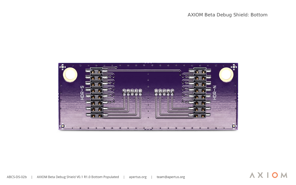
- Compatible with both East and West shield headers.
- Via East shield header has four high-speed LVDS pairs (1Gbit/s).
- Via West shield header has four medium-speed LVDS pairs (200Mb/s+).
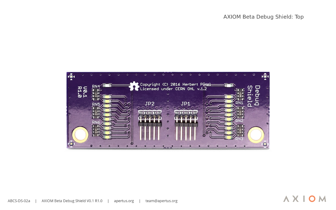
- 20x GPIO bank LED indicators.
- 2x Power LEDS.
- AC coupling and biasing via pull-ups and pull-downs.
- Shields are not hot pluggable.
See Beta Main Board for specifics on how shields are utilised and Camera Structure for an overview on how PCBs are stacked.
Current Revision
https://wiki.apertus.org/index.php/AXIOM_Beta_Debug_Shield_V0.1_R1.0


