Difference between revisions of "Elgato CAM LINK 4K"
| Line 1: | Line 1: | ||
This PCB is relevant to the project because [[AXIOM Beta]] | This PCB is relevant to the project because [[AXIOM Beta]] generates HDMI content inside its [[Beta Main Board]] FPGA and therefore pretty much any data can be sent over an HDMI connection. The problem is there's no way to control the HDMI receiver side - meaning recorder manufacturers do all kinds of strange things with the image (sharpening, color conversions, etc.) and in general only support very specific resolutions/framerates. There are also no standards for HDMI. | ||
With the Elgato CAM Link 4k it's now possible to take over control of the receiver side. | With the Elgato CAM Link 4k it's now possible to take over control of the receiver side. | ||
Revision as of 12:28, 18 December 2019
This PCB is relevant to the project because AXIOM Beta generates HDMI content inside its Beta Main Board FPGA and therefore pretty much any data can be sent over an HDMI connection. The problem is there's no way to control the HDMI receiver side - meaning recorder manufacturers do all kinds of strange things with the image (sharpening, color conversions, etc.) and in general only support very specific resolutions/framerates. There are also no standards for HDMI.
With the Elgato CAM Link 4k it's now possible to take over control of the receiver side.
This opens up a whole world of possibilities with regards to what data could be packed into the HDMI "frame" if it's used as a data container.
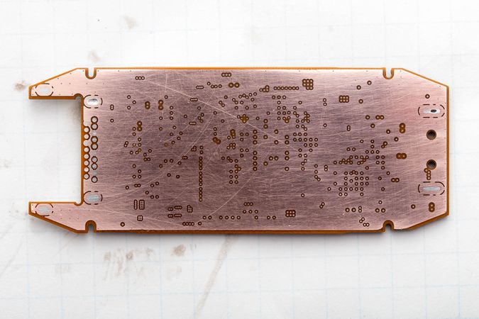
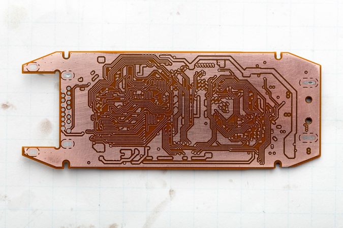
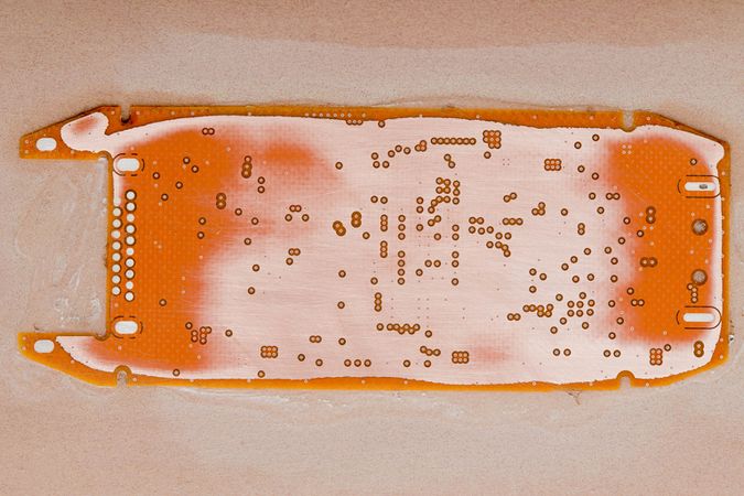
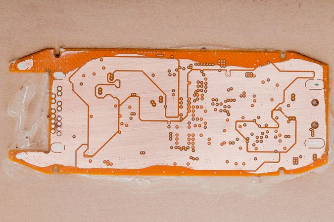
1 PCB
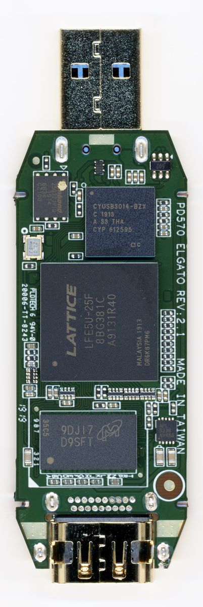
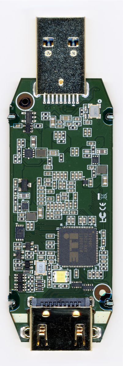
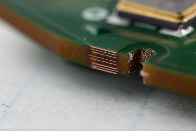
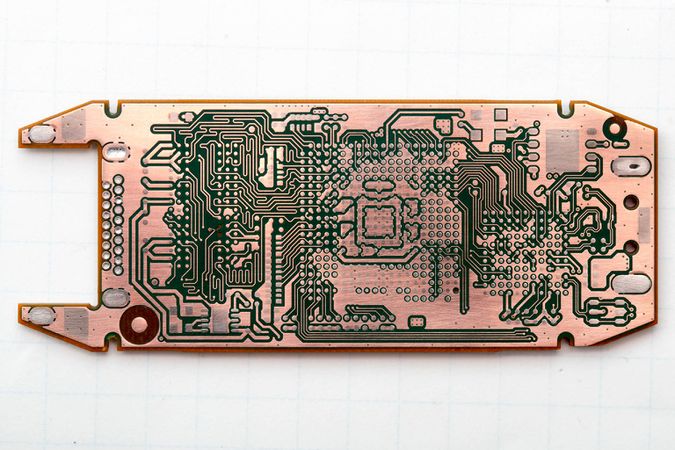
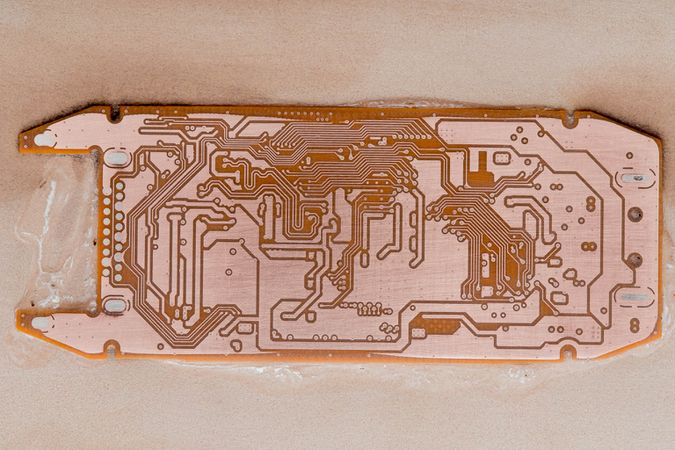
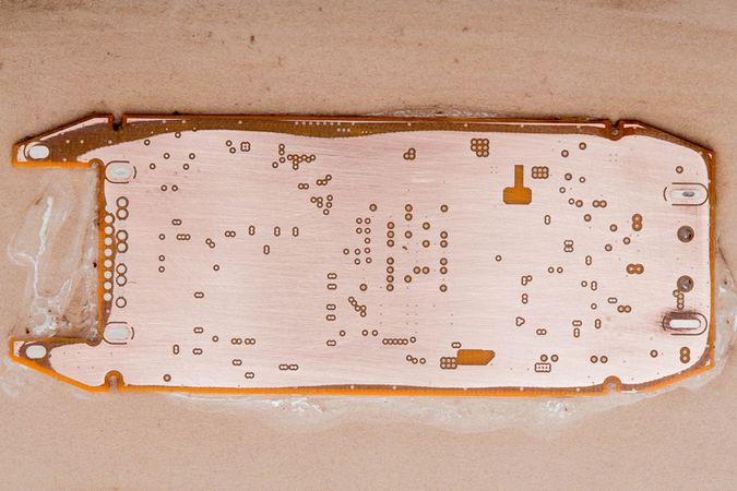
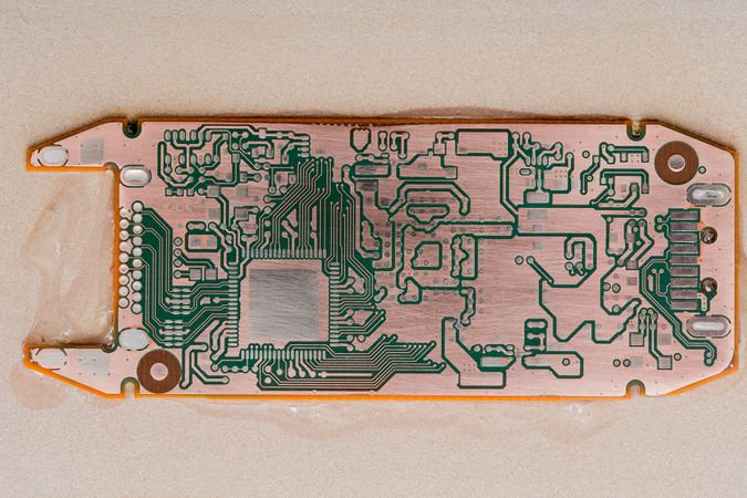
It is reported to be an 8 layer PCB. Probably atleast a 2-3+ HDI.
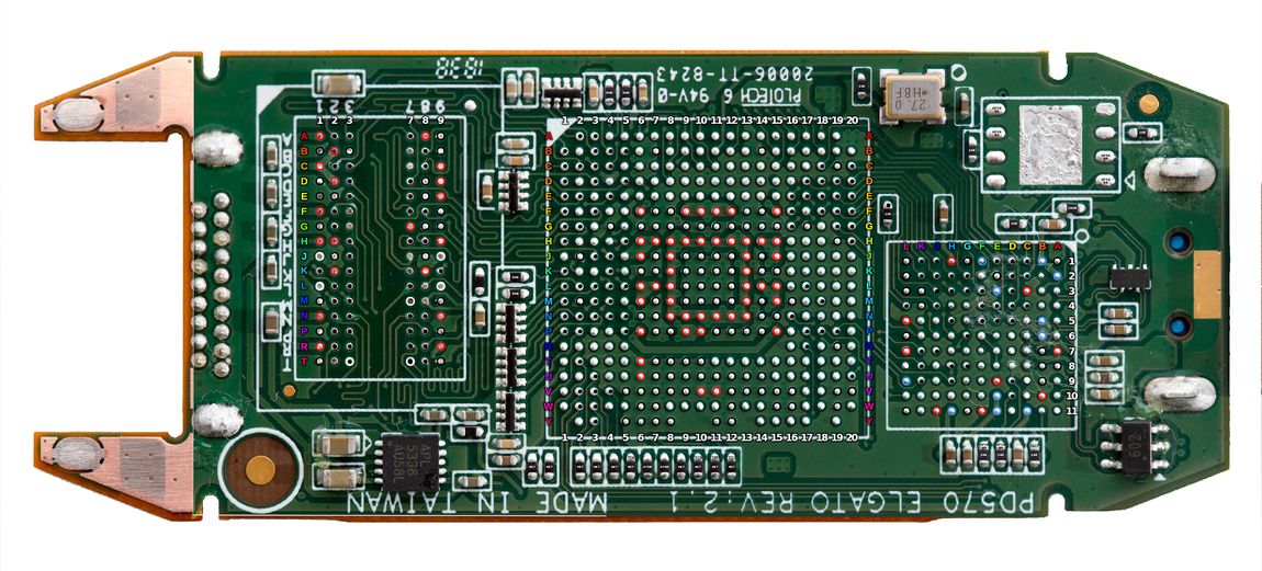
Pinout Mapping (WIP):
2 Firmware
a dump of the SPI communication (and the decoded flash data) can be found here:
- http://vserver.13thfloor.at/Stuff/ELGATO/boot_decode.txt
- http://vserver.13thfloor.at/Stuff/ELGATO/boot.vcd.xz
3 Further files/links
