AXIOM Gamma
1 Project Overview
In the interest of clarity it should be noted as you browse these entries (and those on other pages) that the AXIOM Gamma has been shelved for the time being. This means that, whilst we think there is scope for further development of the camera, this research may not recommence until some way into the future. There are three reasons for this:
- We found that the AXIOM Gamma was going to be very expensive to produce and in-turn purchase.
- It was felt that the AXIOM Beta's potential hadn't been fully realised. In other words, if development was focused on the smaller form factor camera it may one day pave the way for refining software with the AXIOM Gamma in mind, that the Beta could be made far more powerful than we had at first thought.
- It was the AXIOM Beta that had been crowdfunded. This meant that our obligation was to those who backed the Beta's research and development, and to the criteria that the campaign centered around.
2 Initial concept
This concept is still up for discussion.
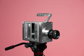
The general goal is/was to revive the "Cat on the Shoulder".
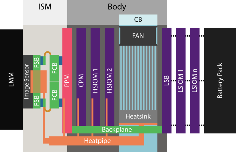
3 Module Block Diagram
4 Optical Modules
4.1 Lens Mount Module (LMM)
4.2 Optical Filter Module (OFM)
Optional.
4.3 Image Sensor Module (ISM)
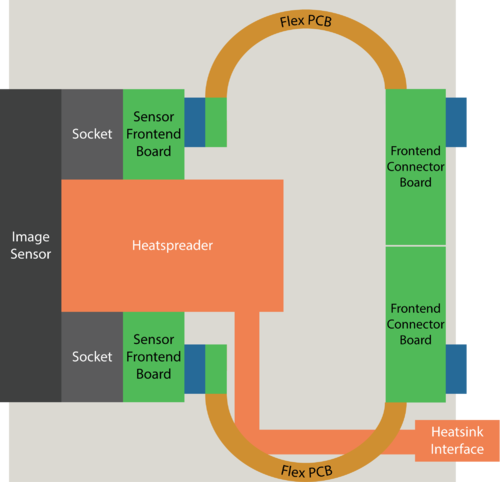
The image sensor in the AXIOM Gamma will be mechanically adjustable in dimensions of flange focal distance (back focus = Z-axis), a shift in XY-axes and XYZ rotation.
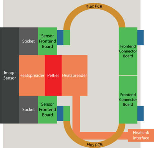
For creating space for the heatpipes and decoupling the image sensor from the rest of the module two rigid-flex PCBs are added to the existing designs. The rigid part of the rigid-flex PCB will be screwed to the back of the module exposing the connectors to the back.
Two cooling options:
- passive: Copper heatpipes
- active: Peltier element behind sensor (see below)
Peltier:
Usage of a Peltier-element proves to be problematic:
High power consumption renders mobile usages inefficient
Power consumption within the Peltier generates more additional heat
Water condensation within the electronics on the cool Peltier side, requirement of sealing -> increased complexity of manufacturing, design, maintenance, repairs, etc.
Conclusion:
Sensor front end module without Peltier element for general usage, one version with Peltier element for people who are aware of the implications and/or for experimentation purposes
4.3.1 Sensor Frontend Board (SFB)
4.3.2 Frontend Connector Board (FCB)
5 Front Module
5.1 Pre-Processing Module (PPM)
Sensor access is implemented by using a Xilinx Kintex-7 160T FPGA.
Captures raw image date from the sensor and responsible for general “raw” processing of the sensel (image sensor pixel) values, e.g. spatial and temporal binning of the raw data if lower resolutions and/or frame rates are desired in subsequent processing steps.
Board-To-Board Connection (B2B)
Finger on backplane and PCIE-164 connector on PPM.
For sensor adjustment a PCIE Riser card can be used to detach the PPM and the ISM from the Body and still access the set screws.
6 Body
6.1 Backplane
Connects PPM, CPM and HSIOMs via high-speed serial links and LSIOM via low-speed links.
Backplane circuitry include the power consumption measurement and management of an external Battery and also hot-plug detection and powering of the modules.
The Backplane contains a muxed JTAG interface to allow debugging of all add-on boards via a central connector.
6.2 Core Processing Module (CPM)
Most likely a Zynq 7030 FPGA + dual ARM core System on Chip (SoC).
6.3 2x High Speed I/O Module Slots (HSIOM)
Also called High Speed Module
Generally used for storage, input or output of high-speed signals. Typical examples would be SSD storage, HDMI/SDI output or SDI input.
For this reason, the HSIOMs have dedicated high-speed access to the preprocessed image data coming from the PPM and the processed Data from the CPM.
Connections are typically 4 lanes, either connected directly or via a high-speed mux. The theoretically achievable data-rate would be 10Gbps per lane (the limit of the mux, allthough the FPGA transceivers are not much faster), but the practically reachable data rate will likely be lower depending on EMI-performance, power-consumption and board losses. For a 4K raw image stream, only a fraction of the theoretical speed is needed.
6.4 Cooling Bay (CB)
Cooling will be done as Module (Central heatsink plus fan).
The backplane needs to account for that as it will have to go “around” the Cooling Bay.
6.5 Low Speed Bridge (LSB)
Finger on backplane and PCIE-164 connector on LSIO Bridge.
7 Stackmodules
Docking to LSB
7.1 Low Speed IO Modules (LSIOM)
No high-speed access to raw image data stream, but are connected to CPM and PPM via multiple LVDS lanes to allow medium-rate traffic (1-2 Gbps total shared across all LSIOMs).
Typical examples: Audio, Timecode, Trigger or Genlock inputs/outputs, Gyroscopes, Accelerometers, GPS modules.
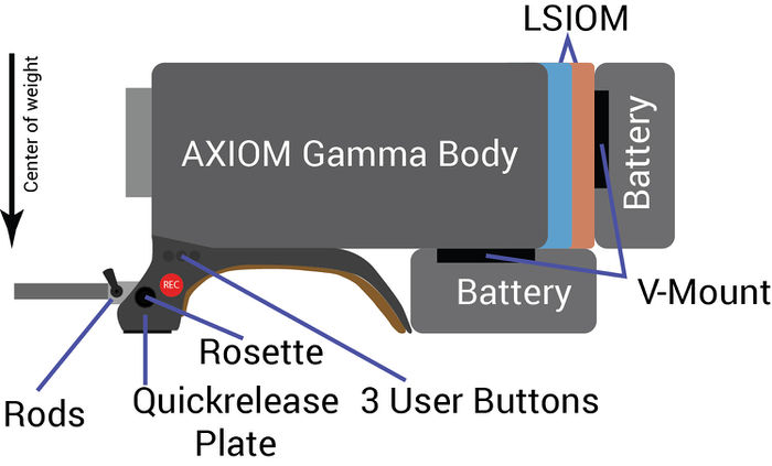
7.2 Battery Mount
Last LSIOM in stack.
8 Software
8.1 Android
8.1.1 Android Hardware
Zynq provides 1080p30 (or 1080p60 if bandwidth allows) stream via four LVDS lanes to a LSIOM with a NVIDIA Tegra K1 chip to further distribute the stream over AOSP, eg. an HDMI to be viewed on an external screen (preferrably with touchscreen support). Communication between Zynq and Tegra happens over Serial Protocol Interface (SPI).
Tegra K1 for encoding to 1080p60, SPI between K1 and Zynq, as Zynq has no GPU to encode on and it would take too much capacities from the CPU on dedicated LSIOM.
For faster prototyping, several readymade modules can be used: - made by GE (too expensive) - made by Toradex (Open Source baseboard)
To save up bandwidth on the lanes themselves and processing power of the Zynq, another possibility would be a dedicated raw stream to the Android module and debayer it with CUDA/OpenGL.
8.1.2 Android Software
As the Zynq will generate a scaled down 1080p30 version of the sensor image, it will also be sent to a new LSIOM running AOSP with an Transition-Minimized Differential Signaling (TMDS), preferably HDMI.
The 1080p signal would take up approximately four LVDS data lanes.
The downscaled stream from the Zynq fakes being a standard camera, but without direct controls. Sensor configuration should always be done via Zynq. A partial sensor control will be achieved via a SPI connection between K1 and Zynq.
8.2 Deliverables
D1.3 Ecosystem Launch - University Applied Arts Vienna
D1.4 Data Management Plan - University Applied Arts Vienna
D2.1 ISFES Hardware Design - af inventions
D2.2 ISFES Hardware Manufacturing - apertus°
D2.3 ISFES Software - Antmicro V2
D3.1 IPS Hardware Design - af inventions V2
D3.2 IPS Power Supply Hardware - af inventions V2
D3.3 IPS Hardware Manufacturing - apertus° V2
D3.4 IPS Software - Antmicro V2
D5.1 IOIS Hardware Design - af inventions V2
D5.2 IOIS Hardware Manufacturing - apertus° V2
D5.3 IOIS Software - Antmicro V2
D6.1 CELM Enclosure Design - Denz V2
D6.2 CELM Lens Design - Denz V2
This page is work in progress.
8.3 Mandatory on all publications
This project has received funding from the European Union’s Horizon 2020 research and innovation programme under grant agreement No 645560
