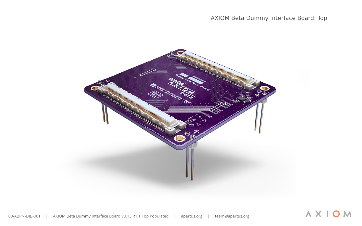
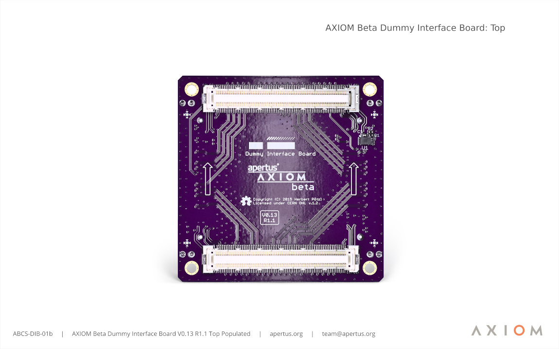
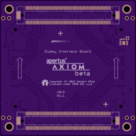
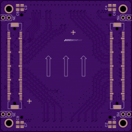
Beta Interface Dummy Board
The AXIOM Beta Dummy Interface Board acts as a bridge between the Image Sensor Board and the rest of the camera. It connects the LVDS pairs from the Main Board with the Image Sensor Board. Capacitors to smooth-out power ripples and provide buffering have also been incorporated. It should be noted that this printed circuit board is extremely specific to the CMV12000 image sensor.
Note: The present iteration of Interface Board limits image sensor throughput to 150FPS@4K. This current Beta Interface Dummy Board connects 32+3 of the 64+3 LVDS channels available in the CMV12000. A 'Smart Sensor Interface Board', however, would allow the camera to get 4K@300 FPS into the pipeline. High speed memory on this board would allow buffering of images for high speed recording bursts or temporal binning/averaging and thus allow for use of the microzed with output being slower than acquisition bandwidths. Requires 400+ IO so XC7A200T FBG676 FPGA which is 200+€ is the only option (covered by webpack license though). Herbert has done a few tests to see if it would be possible to do with OSHpark stackups and the conclusion was: doable but non-trivial. The general design is rather straight forward (connect 36 LVDS pairs on one end and 80 LVDS pairs on the other end to an FPGA). But it is also completely unknown how much processing can be done there and what that means for cooling, etc (not only the MicroZed, but the Beta Interface Board itself will also heat up). The simplest application is the 'gearwork' between SB and MB. It could also run a sensor emulation eliminating the SFE for many development task and/or testing. It could do fancy stuff with the sensor data (preprocessing).
If you'd like to assist with development in this area please make contact.
Revisions
Current:
axiom beta interface dummy v0.13
Archive:
axiom beta interface dummy v0.9


