KiCAD Evaluation
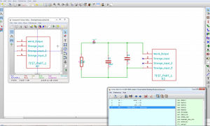
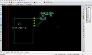
KiCAD is a FLOSS software to create schematics and PCB layouts (EDA) and a candidate for being used to create all future Axiom/Alpha electronic designs.
Official KiCAD website: http://www.kicad-pcb.org/display/KICAD/KiCad+EDA+Software+Suite
We are currently evaluating if it can really meet the high demands of this complex kind of designs we plan to do.
As interesting sidenode: people from CERN are planning to push KiCAD forward with a list of wishes and improvements: http://www.ohwr.org/projects/ohr-meta/wiki/Foss-pcb
1 Glossary
component = a symbol of a part in the schematic viewer
footprint = Module = a physical part (eg. chip) in the PCB layout editor
netlist = basically a file (*.net) that lists all connections from each component's pin to another one. Used to connect schematic and board together plus a component/footprint association file (*.cmp)
2 Tips
- To switch from dark to bright schematic editor (much easier to look at) go to Preferences -> Colors and click Background Color: White
- enable smooth drag/drop like view panning with middle mouse buttons under Preferences
- Working with multiple components in a single device: http://kicadhowto.wikidot.com/co1compmg and http://kicadhowto.wikidot.com/sk1qn1
3 Guides/Tutorials
The perfect way to get to know the basics of the software are these 2 youtube videos (if you can live with the the electronic stephen hawking voice):
- Tutorial part 1: http://www.youtube.com/watch?v=rkQ0nVX1q1k
- Tutorial part 2: http://www.youtube.com/watch?v=8HNMihqa844
- Creating new components for KiCAD: http://store.curiousinventor.com/guides/kicad/new_components/
More Tutorials on:
3.1 Typical Workflow
- Build schematic
- Annotate components
- Export netlist
- Choose footprint for each component
- import netlist with component list into PCB editor
3.2 Creating custom components and footprints
Creating new custom components and footprints is pretty straight forward and works fine with the integrated editors.
3.3 What other people are thinking
The folks over at http://dangerousprototypes.com/2012/09/14/dangerous-prototypes-kicad-eda-experience/ listed their observations:
- no screen panning with middle mouse button <- actually you can pan with the middle mouse button but rather than a kind of drag/drop shifting of the view you center the view where you click. Alternatively you can enable smooth drag/drop like panning with middle mouse buttons under Preferences (its disabled by default)
- "Minor adjustments to a schematic after starting the board are a nightmare. You have to create a new netlist, loading it into the PCB editor, and update the PCB connections. This gets very tedious with our team-based iterative design process." <- "As many issues as I have with KiCad, I don’t think changing the schematic is nearly as bad as you say. After changing the schematic you just have to run Annotate, making sure “Keep existing annotation” is selected. If you haven’t changed or added footprints, it’s now enough to click “Read netlist” in the PCB editor, and your changes will show up."
- Placing vias on polygons/planes is too complicated, such as vias to join ground planes. You have to trace each via to an already existing trace or pad and connect to it.
- Another thing to note is that KiCad doesn’t have a command console. Placing components at exact coordinates is rather complicated, and requires frequent grid alterations.
- When I update a netlist which has different trace rules and some of those are assigned to numerical nets. Because the PCB tool doesn’t know these are different nets now it doesn’t keep the categories straight. You can of course give your own labels to all the wires and it would keep it straight but that’s a bit tedious.
4 Alternatives
- Free version of Eagle for non commercial use only and with size restrictions.
- gEDA is really a big electrical design tool suite that happens to do PCBs as such it isn’t all that integrated, this makes it harder to use than KiCAD. (quoting http://teholabs.com/knowledge/kicad.html)

