Difference between revisions of "Beta Main Board"
From apertus wiki
m |
m |
||
| Line 1: | Line 1: | ||
[[File:BetaMainboard 0.32 TOP.jpg | thumb | 500px | PCB Top with components]] | [[File:BetaMainboard 0.32 TOP.jpg | thumb | 500px | PCB Top with components]] | ||
[[File:BetaMainboard 0.32 BOTTOM.jpg | thumb | 500px | PCB Bottom with components.]] | |||
=About= | =About= | ||
| Line 11: | Line 12: | ||
<gallery mode="packed" heights="180"> | <gallery mode="packed" heights="180"> | ||
Image:Top.png| PCB Top. | Image:Top.png| PCB Top. | ||
Image:Bottom.png| PCB Bottom. | Image:Bottom.png| PCB Bottom. | ||
Revision as of 15:58, 16 January 2018


1 About
The Beta Mainboard deals with interfacing the plugin modules and shields and therefore acts as a kind of data crossroad.
It features two Beta CSO slots - one on each PCB side - directly behind the image sensor center. This is intended for IMU sensors or future extensions.
The purpose of the two Lattice FPGAs (the so called routing fabrics) is to handle all the low speed GPIO stuff required for plugin modules, shields and CSO without sacrificing valuable Zynq GPIOs.
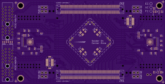
PCB Top.
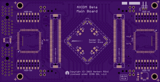
PCB Bottom.


1.1 Revisions
Current:
AXIOM Beta Main Board V0.36 R1.2
Archive:
axiom beta board 100 v0.15 test