Difference between revisions of "Elgato CAM LINK 4K"
From apertus wiki
| Line 1: | Line 1: | ||
==PCB== | |||
<gallery mode="packed" heights="800"> | <gallery mode="packed" heights="800"> | ||
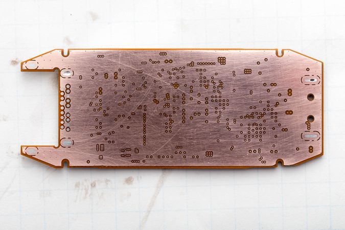
Image:Elgato cam link 4k side a.jpg | PCB Side 1. | Image:Elgato cam link 4k side a.jpg | PCB Side 1. | ||
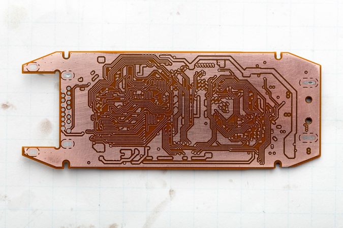
Image:Elgato cam link 4k side b.jpg| PCB Side 2 (mirrored). | Image:Elgato cam link 4k side b.jpg| PCB Side 2 (mirrored). | ||
</gallery> | </gallery> | ||
It is reported to be an 8 layer PCB. Probably atleast a 2-3+ HDI. | |||
<gallery mode="packed" heights="300"> | |||
Image:8layers.jpg | PCB Side View | |||
Image:Layer0.jpg | PCB Layer 1/8 | |||
Image:IMG_7370-2.jpg| PCB Layer 2/8 | |||
Image:IMG_7379.jpg| PCB Layer 3/8 | |||
</gallery> | |||
Credit: https://twitter.com/GregDavill | |||
'''Pinout Mapping (WIP):''' | |||
[[File:Layers-pinout.jpg | 1150px]] | |||
https://docs.google.com/spreadsheets/d/17SmOY7Npzz2Hj1kz4DWKzrBAl0PYMWU085NeT3AY0D4/edit#gid=0 | |||
==Firmware== | |||
a dump of the SPI communication (and the decoded flash data) can be found here: | a dump of the SPI communication (and the decoded flash data) can be found here: | ||
Revision as of 11:10, 15 December 2019
1 PCB
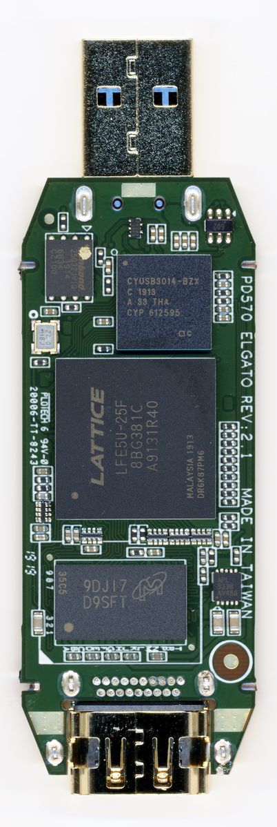
PCB Side 1.
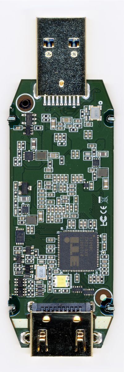
PCB Side 2 (mirrored).


It is reported to be an 8 layer PCB. Probably atleast a 2-3+ HDI.
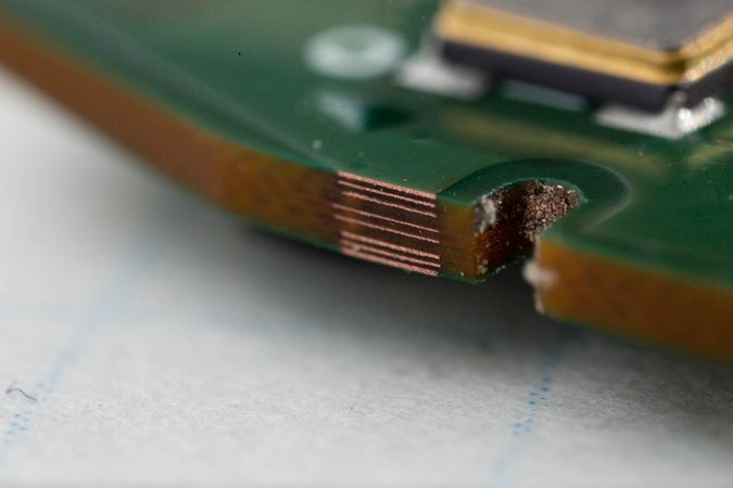
PCB Side View
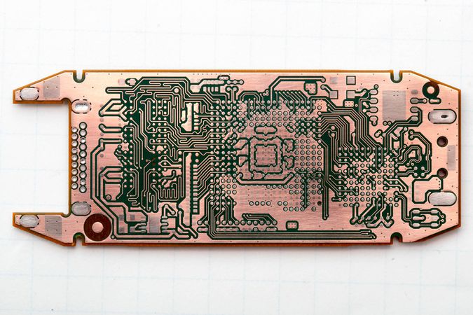
PCB Layer 1/8
PCB Layer 2/8
PCB Layer 3/8


Credit: https://twitter.com/GregDavill
Pinout Mapping (WIP):

https://docs.google.com/spreadsheets/d/17SmOY7Npzz2Hj1kz4DWKzrBAl0PYMWU085NeT3AY0D4/edit#gid=0
2 Firmware
a dump of the SPI communication (and the decoded flash data) can be found here: