Difference between revisions of "Elgato CAM LINK 4K"
| Line 12: | Line 12: | ||
Image:IMG_7370-2.jpg| PCB Layer 2/8 | Image:IMG_7370-2.jpg| PCB Layer 2/8 | ||
Image:IMG_7379.jpg| PCB Layer 3/8 | Image:IMG_7379.jpg| PCB Layer 3/8 | ||
Image:EL_BfhqUEAUWij4.jpg| PCB Layer 4/8 (Now from the back, flipped for ease of alignment.) Another solid ground plane. | |||
Image:EL_BtC0U0AAkf_0.jpg| PCB Layer 5/8 (flipped) Power planes. | |||
Image:EL_CFf6U8AEk_H6.jpg| PCB Layer 6/8 (flipped) Two sneaky DDR memory pairs routed on this layer. | |||
Image:EL_CdWzU8AEtWR_.jpg| PCB Layer 7/8 (flipped) ground plane - Note: 2 cutouts in this plane, that seem to correspond to SW signals of DCDC buck converters. I've never seen that before? Maybe to reduce capacitance on the SW pin? | |||
Image:EL_CnZjUwAEaASg.jpg| PCB Layer 8/8 (flipped) bottom layer | |||
</gallery> | </gallery> | ||
Revision as of 12:25, 17 December 2019
1 PCB
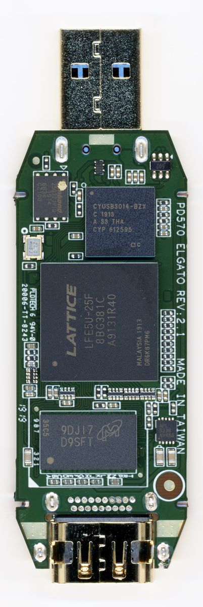
PCB Side 1.
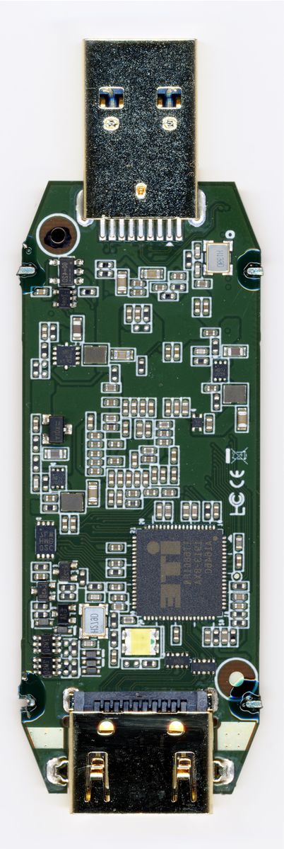
PCB Side 2 (mirrored).


It is reported to be an 8 layer PCB. Probably atleast a 2-3+ HDI.
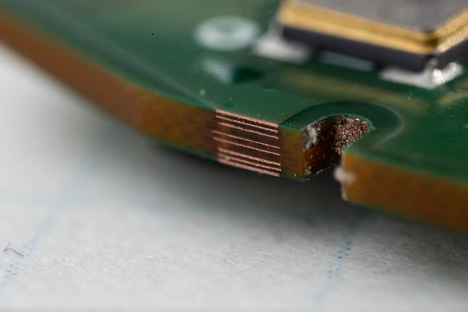
PCB Side View
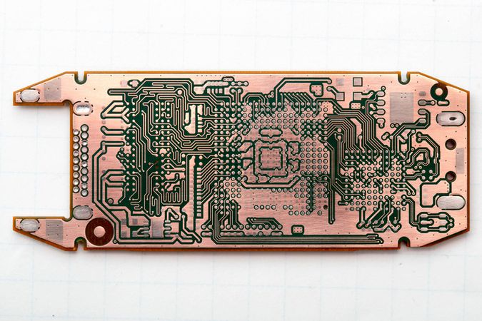
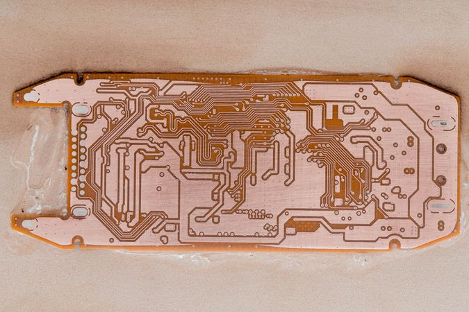
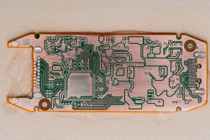
PCB Layer 1/8
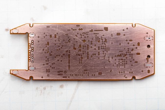
PCB Layer 2/8
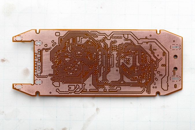
PCB Layer 3/8
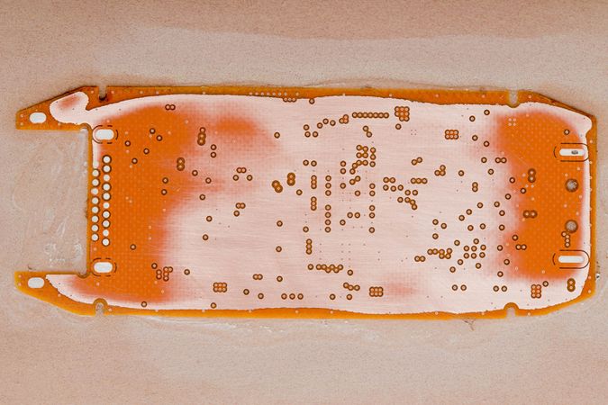
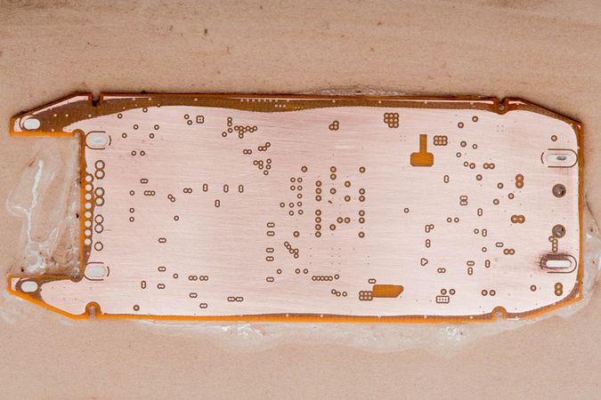
PCB Layer 4/8 (Now from the back, flipped for ease of alignment.) Another solid ground plane.
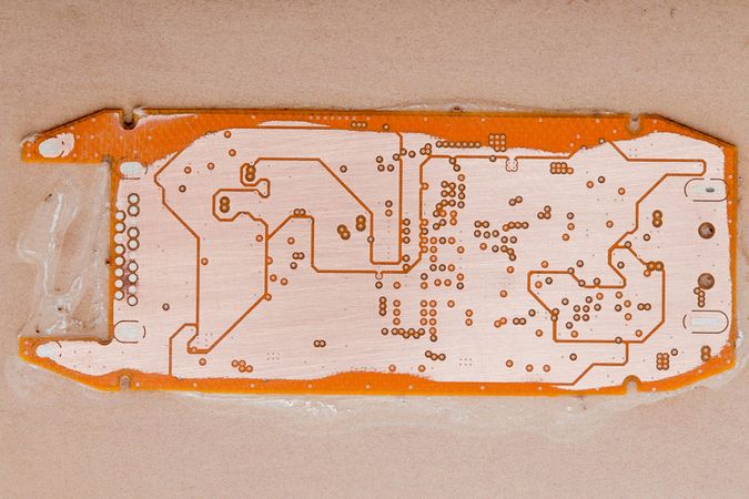
PCB Layer 5/8 (flipped) Power planes.
PCB Layer 6/8 (flipped) Two sneaky DDR memory pairs routed on this layer.
PCB Layer 7/8 (flipped) ground plane - Note: 2 cutouts in this plane, that seem to correspond to SW signals of DCDC buck converters. I've never seen that before? Maybe to reduce capacitance on the SW pin?
PCB Layer 8/8 (flipped) bottom layer


Credit: https://twitter.com/GregDavill
Pinout Mapping (WIP):

https://docs.google.com/spreadsheets/d/17SmOY7Npzz2Hj1kz4DWKzrBAl0PYMWU085NeT3AY0D4/edit#gid=0
2 Firmware
a dump of the SPI communication (and the decoded flash data) can be found here:
http://vserver.13thfloor.at/Stuff/ELGATO/boot_decode.txt
http://vserver.13thfloor.at/Stuff/ELGATO/boot.vcd.xz
Further files/links: