Beta Power Board

1 About
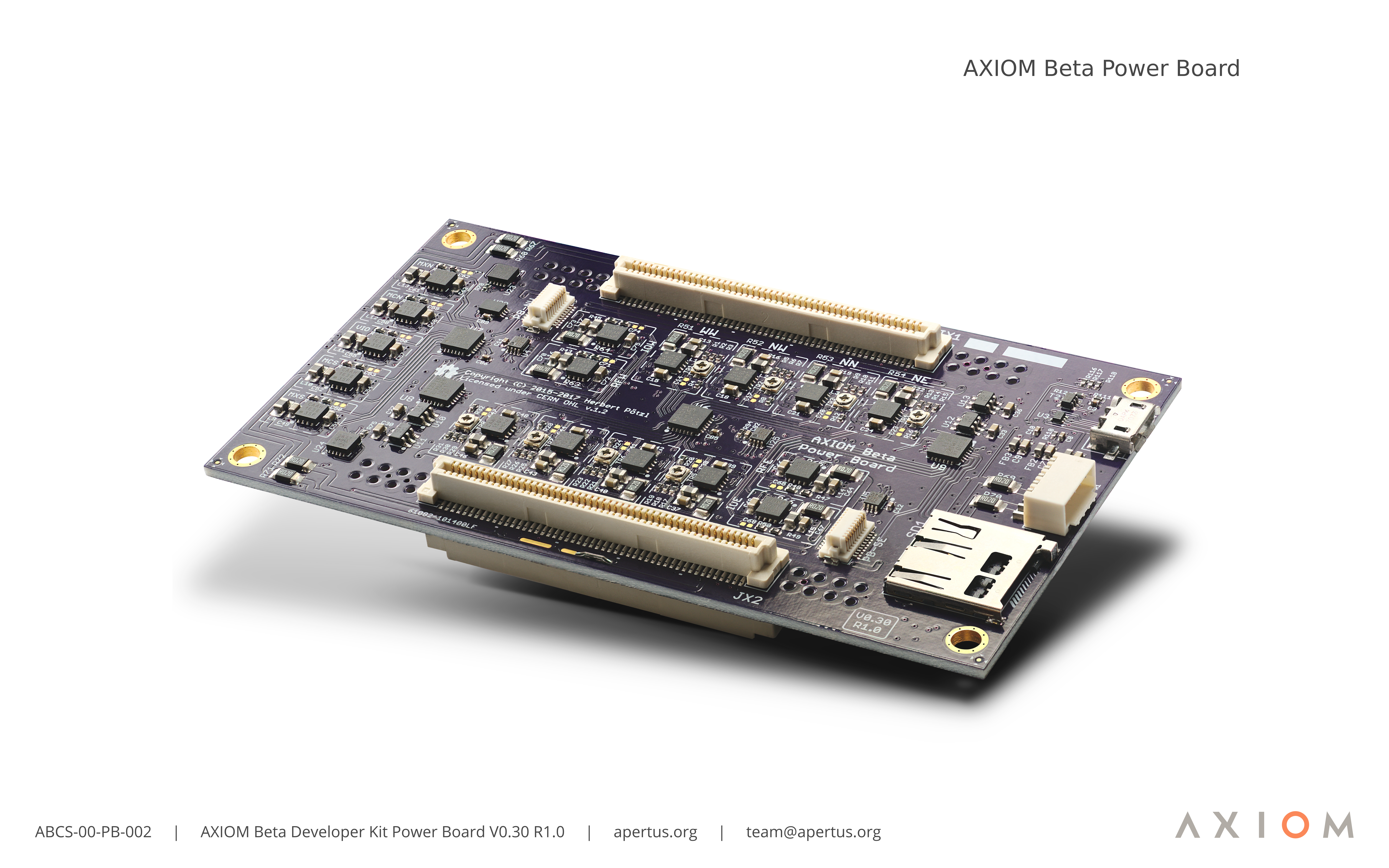
The AXIOM Beta Power Board sits between the Beta Main Board and the MicroZed™ in the camera's PCB stack. It generates all the different supply voltages for the chips and logic on the other PCB’s inside the camera. It also monitors currents so that it can estimate remaining power based on the recorded consumption. Version 1 of the Beta Power Board has the 8 different voltage rails calibrated at factory. In case of a future hardware upgrade that require any power rail to have a different reference voltage this calibration needs to be redone.
2 Features
Comprehensives list of features for currently available board versions.
2.1 V0.30
- Nine high-current (1.5A) low-dropout (LDO) linear regulators for IO, Voltages on MicroZed, Center Solder-on-Area (CSO), Main Board routing, Fabrics (RF) for plugin modules and shields.
- Eight high-current-adjustable LDOs for Interface Board (2) and sensor front-end (6) power rails.
- Ten low-current regulators for Main Board bus power (I2C, SPI, JTAG) and CSO Supply.
- Extensive instrumentation to monitor power (Voltage and Current) and control all Power Rails.
- USB (FT232 based) debug interface (JTAG).
- 512 Byte EEPROM for Identification and Configuration Information.
- Temperature Monitoring.
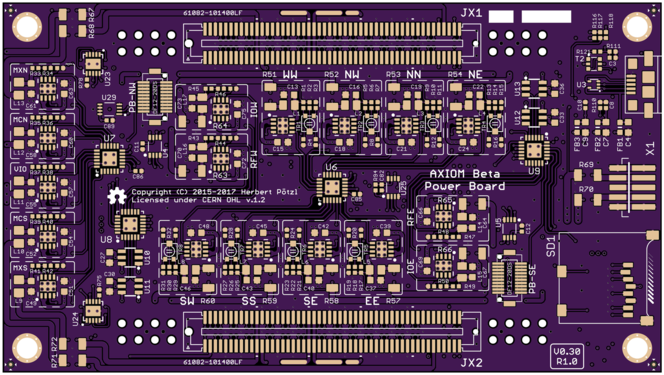
Power Board V0.30 PCB Top.
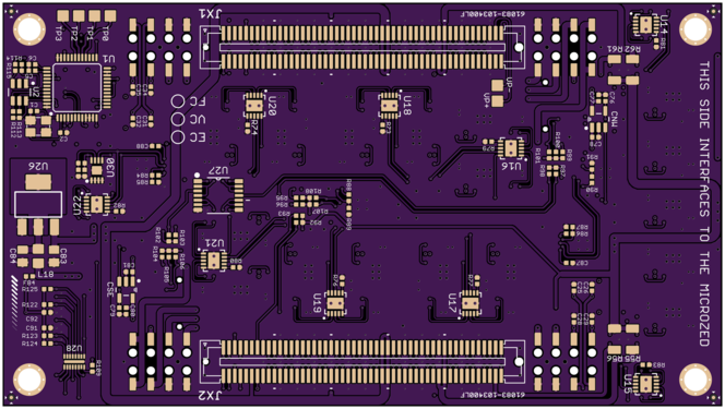
Power Board V0.30 PCB Bottom.


2.2 Features for V0.37 (to become V1.0)
- 5V Input
- Dual 3A step-down converter for optional increased input range (6-17V). Software still needs to be written.
- Always-on low-power controller (MCU) for the two main power supply rails with input voltage monitoring, power button and fan interface.
- Nine high current (1.5A) low dropout (LDO) linear regulators for IO voltages on MicroZed, Center Solder-on-Area (CSO) and Main Board routing fabrics (RF), Plugin modules and Shields.
- Eight high-current-adjustable LDOs for Interface Board (2) and sensor front-end (6) power pails.
- Ten low-current regulators for Main Board bus power (I2C, SPI, JTAG) and CSO supply.
- Extensive instrumentation to monitor power (voltage and current) and control all power rails.
- Voltage level conversion for primary and secondary system management bus.
- Unique ID and 128 Byte user-flash for configuration information.
- Secondary SD card Interface.
- Dual temperature monitoring.
2.3 Planned features for V2
- Over-and-under voltage protection for input rails.
- Always-on low-power controller (MCU) for the two main power supply rails.
- Sixteen digitally configurable high current (2A) switching regulators for IO Voltages on MicroZed, Center Solder-on-Area (CSO) and Main Board routing fabrics (RF), plugin modules and shields.
- USB (PIC based) debug and monitoring interface.
- Eight digitally configurable high-current (3A) switching regulators for Interface Board (2) and Sensor Front-end (6) power rails.
- Fourteen low-current regulators for Main Board bus power (I2C, SPI, JTAG) and CSO supply.
- Precision instrumentation to monitor power (voltage and current) and control all power rails.
- Distributed event-based power control system with direct feedback loop.
- Diagnostics RGB LED and power button.
- Unique ID and 128 Byte user-flash for configuration information.
- External power button, fan and communication interface.
- Secondary SD card interface.
- Advanced temperature monitoring.
Structural changes:
- DC barrel connector attached directly to the PB with a cable.
- mechanical trimmer (discontinued) replacement -> switching regulators with digital voltage control.
- PICO SPOX power input connector will be moved "into" the PB so the cable can be routed inside the camera enclosure towards the backside.
- RGB LED and push-button (ALPS SKSNLAE010 currently considered) moved from smart power adapter to PB (top side, north east).
- Connector for extension PCB (RGB LED, buttons, FAN control) and legacy FAN control (moved from Main Board).
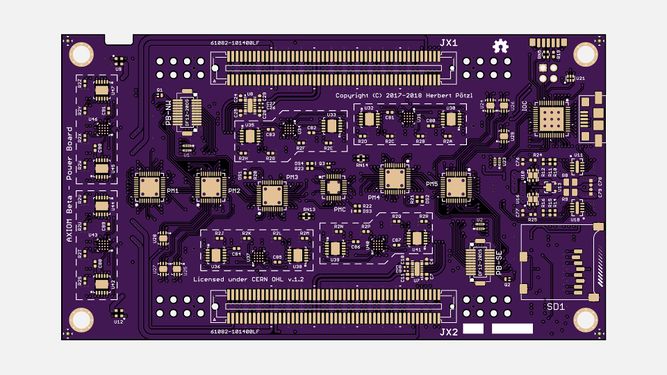
Power Board V2.23 PCB Top.
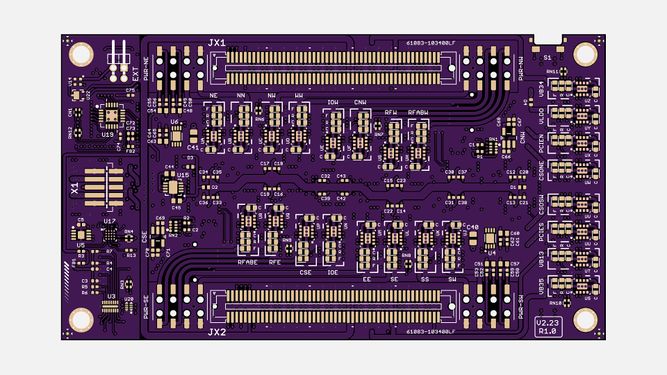
Power Board V2.23 PCB Bottom.


3 Revisions
Sources: https://apertus-open-source-cinema.github.io/pcbs/index.html#/boards/AXIOM%20Beta%20Power%20Board/
Current:
Archive:
- AXIOM Beta Power Board v0.25
- axiom beta power board v0.23
- axiom beta power board v0.22 test
- axiom beta power board v0.17 test
- axiom beta power board v0.11 test
- axiom beta power board v0.8 test
- axiom beta power board v0.9 test
4 Calibrating Voltages
This describes the process required when factory assembling the power board hardware in the AXIOM Beta stack.
./power_init.sh
./power_on.sh
Wait for a bit.
./pac1720_info.sh
This will output something like:
ZED_5V          4.8828 V [1f40]         +10.1562 mV [104]   +677.08 mA
BETA_5V         4.8828 V [1f40]          +1.2891 mV [021]    +85.94 mA
HDN             3.2812 V [1500]          +0.0000 mV [000]     +0.00 mA
PCIE_N_V        3.2422 V [14c0]          +0.0000 mV [000]     +0.00 mA
HDS             3.2031 V [1480]          +0.0000 mV [000]     +0.00 mA
PCIE_S_V        3.2422 V [14c0]          +0.0000 mV [000]     +0.00 mA
RFW_V           3.2422 V [14c0]          -0.0391 mV [fff]     -2.60 mA
IOW_V           3.2617 V [14e0]          +0.0000 mV [000]     +0.00 mA
RFE_V           3.2422 V [14c0]          +0.0000 mV [000]     +0.00 mA
IOE_V           3.2812 V [1500]          +0.0000 mV [000]     +0.00 mA
VCCO_35         2.4219 V [ f80]          -0.0391 mV [fff]     -2.60 mA
VCCO_13         2.4609 V [ fc0]          +0.0000 mV [000]     +0.00 mA
PCIE_IO         2.4609 V [ fc0]          -0.0781 mV [ffe]     -5.21 mA
VCCO_34         2.4609 V [ fc0]          +0.9766 mV [019]    +65.10 mA
W_VW            2.7734 V [11c0]          +0.0000 mV [000]     +0.00 mA
N_VW            2.8125 V [1200]          +0.0000 mV [000]     +0.00 mA
N_VN            2.7734 V [11c0]          -0.0391 mV [fff]     -2.60 mA
N_VE            2.8516 V [1240]          +0.0000 mV [000]     +0.00 mA
E_VE            2.6953 V [1140]          -0.0391 mV [fff]     -2.60 mA
S_VE            2.8516 V [1240]          +0.0000 mV [000]     +0.00 mA
S_VS            2.7344 V [1180]          -0.0391 mV [fff]     -2.60 mA
S_VW            2.8516 V [1240]          -0.0781 mV [ffe]     -5.21 mA
now run:
watch -n 0.2 ./pac1720_info.sh
which will display the voltages in a clear screen and constantly update the values until you press CTRL+C
The PCB labels and the labels in the CLI correspond like the following:
WW = W_VW
NW = N_VW
NN = N_VN
NE = N_VE
SW = S_VW
SS = S_VS
SE = S_VE
EE = E_VE
Use a tiny screwdriver and adjust the trimmers on the PCB until your values look like this:
W_VW          	2.4609 V [ fc0] 	 -0.0391 mV [fff]     -2.60 mA
N_VW          	3.2422 V [14c0] 	 +0.0000 mV [000]     +0.00 mA
N_VN          	1.8750 V [ c00] 	 -0.0391 mV [fff]     -2.60 mA
N_VE          	3.2617 V [14e0] 	 +0.0000 mV [000]     +0.00 mA
E_VE          	3.2812 V [1500] 	 +0.0391 mV [001]     +2.60 mA
S_VE          	1.9922 V [ cc0] 	 +0.0000 mV [000]     +0.00 mA
S_VS          	2.9883 V [1320] 	 -0.0391 mV [fff]     -2.60 mA
S_VW          	1.9531 V [ c80] 	 -0.1172 mV [ffd]     -7.81 mA