Beta Main Board

The Beta Main Board can be seen as an equivalent of a PC's motherboard. It hosts two external medium-speed shield connectors and two high-speed plugin module slot connectors. These act as a central switch for defining where data captured by the sensor and other interfaces gets routed to inside the hardware. In this regard, all specifics can be dynamically reconfigured in software.

In the centre of the Beta Main Board a 'solder-on' area for Beta CSO slots has been incorporated on both PCB sides. CSOs can for example host chips capable of sensing the camera's orientation and acceleration (the same chips used to stabilise quadcopters and track head movements in VR headsets). Being situated directly behind the image sensor centre means that these sensors are ideally positioned to supply data for image stabilisation or metadata about the camera’s orientation and movement during a shot.

The Beta Main Board is between the Interface Board and the Power Board in the cameras PCB stack.
The purpose of the two Lattice FPGAs (the so called routing fabrics) is to handle all the low speed GPIO stuff required for plugin modules, shields and CSO without sacrificing valuable Zynq GPIOs.
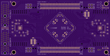
PCB Top.
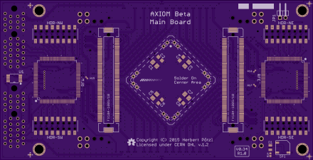
PCB Bottom.


Revisions
Current:
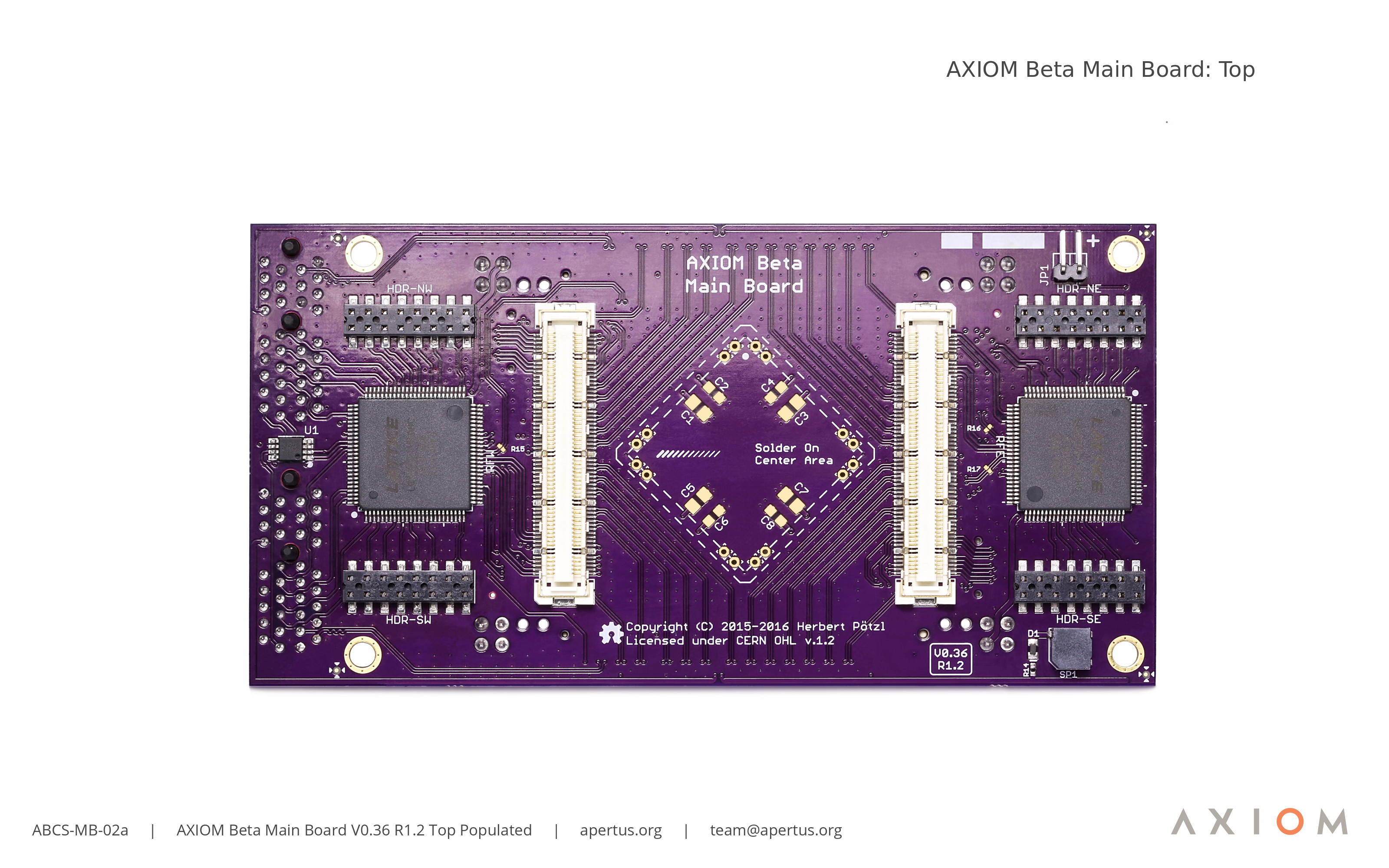
AXIOM Beta Main Board V0.36 R1.2
Archive:
axiom beta board 100 v0.15 test